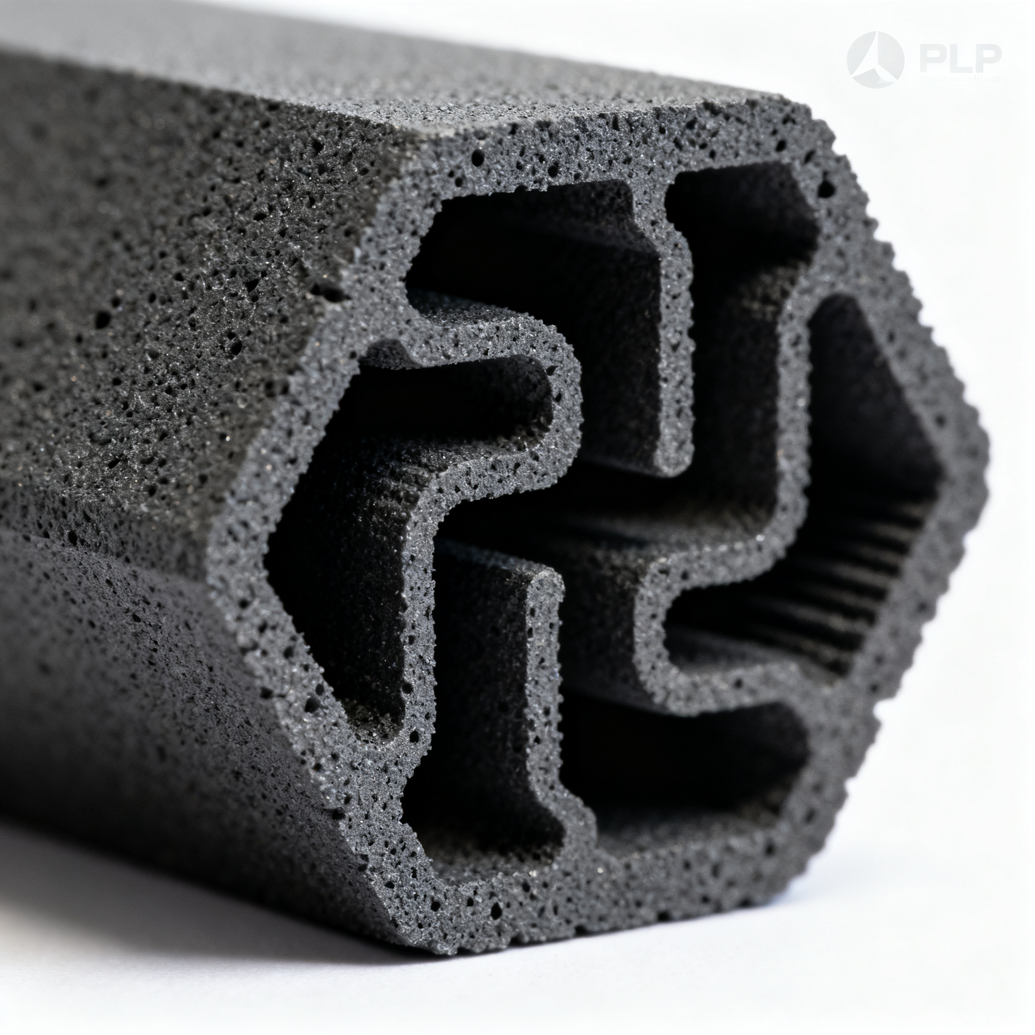
Half-millimeter cooling
In next-generation electronic devices, where every watt counts and space is measured in fractions of a millimeter, thermal management is becoming the real bottleneck. A new photocurable ceramic slurry formulation promises to 3D print structures with cooling channels as thin as 0.2 mm, opening unprecedented scenarios for integrated heat sinks, wafer tables, and water-cooled laser mirrors.
The patent focuses on a concrete problem: in traditional ceramic components with internal channels, two halves are bonded with silicon carbide-based adhesives. During sintering, small amounts of extruded glue clog the channels. If the channel is 5-10 mm wide, the problem is manageable. Below one millimeter, it becomes critical.
The hidden revolution in 0.2 mm channels
A new ceramic slurry formulation makes it possible to 3D print structures with internal channels thinner than ever before, eliminating the limitations of traditional bonding-based production.
The patented slurry contains from 50 to 70% by weight of opaque ceramic particles, from 30 to 50% of photocurable resin, and from 0.3 to 1% of dispersing agent. The latter ingredient is the real turning point: it promotes light penetration into the opaque material, allowing uniform polymerization even in the presence of high ceramic concentrations.
The process uses Digital Light Processing (DLP) technology, already widespread in the industry. A screen projects the image of each layer onto the slurry vat, solidifying the material point by point. The build platform rises, a new layer of slurry is spread, and the cycle repeats.
- 50-70% opaque ceramic particles (silicon carbide)
- 30-50% photopolymerizable resin
- 0.3-1% dispersing agent for light penetration
After printing, the green component is cleaned, subjected to debinding to remove the polymers, and finally sintered or reaction-bonded. The result is a monolithic ceramic body with internal channels ranging in size from 0.2 to 5 mm, without joints or adhesive residue.
Goodbye adhesives, here's how it works
The technology eliminates the problem of channel clogging caused by adhesive extrusion during sintering, a critical limitation in components with ultra-thin features.
In the traditional process, two green preforms are machined with surface channels, joined with SiC-based glue, and then sintered. The assembly pressure inevitably pushes small amounts of adhesive into the channels. With dimensions greater than 5 mm, the problem is marginal. Below 1 mm, a bead of glue can drastically reduce the cross-section or completely block the passage.
The new approach builds the component in a single piece, layer by layer. There are no joining surfaces, there is no glue, there is no risk of extrusion. The channels are defined directly in the CAD file and reproduced precisely in the print.
Manufacturing process
- DLP printing: The slurry is polymerized layer by layer according to the CAD model.
- Cleaning: Removal of unpolymerized slurry from the surface and internal channels.
- Debinding: Thermal removal of organic polymers.
- Sintering or reaction: Final densification of the ceramic body.
The patent cites concrete applications: wafer tables with integrated cooling channels, mirrors for water-cooled collectors, mirrors for high-energy lasers, and micro-coolers for electronic devices. In all these cases, the ability to create thin and complex channels translates into greater thermal efficiency and a smaller footprint.
Trade-offs and real limitations
Despite the advantages, uncertainties remain regarding the stability of the slurry over time and the scalability of the process to high production volumes.
The patent does not provide data on the shelf life of the slurry in storage. High-concentration ceramic suspensions tend to settle or form aggregates over time, requiring agitation or reconditioning before use. It is unclear how long the slurry maintains optimal rheological and photopolymerization properties.
Industrial scalability also remains to be demonstrated. DLP technology is mature for prototypes and small series, but build volumes are limited compared with processes such as binder jetting or pressing. The patent does not specify printing times, cost per part, or direct comparisons with traditional methods on production batches.
The patent does not clarify the long-term stability of the slurry, nor does it provide data on production costs and times compared with traditional methods. Scalability to industrial volumes remains an unknown.
Another critical aspect is the corrosion resistance and thermal conductivity of the finished components. The patent mentions that glass bonding methods, alternatives to SiC adhesive, have poor corrosion resistance and low conductivity. However, no quantitative comparison is provided between the properties of the printed material and those of traditional reaction-bonded components.
How much we really missed it
Direct integration with existing systems such as micro-coolers and wafer tables shows that the technology was designed to enter current production flows.
The patent explicitly cites components already used in the semiconductor and photonics industries: water-cooled wafer tables, micro-coolers for electronic devices, mirrors for high-energy lasers. These products already exist, but they are made using methods that limit geometric complexity and channel miniaturization.
The ability to directly print 0.2 mm channels opens up concrete room for improvement. In micro-coolers, thinner and more numerous channels increase the heat exchange surface without increasing the footprint. In wafer tables, a denser cooling network improves thermal uniformity, reducing deformation and increasing process precision.
| Application | Traditional channel size | DLP channel size |
|---|---|---|
| Wafer tables | 5-10 mm | 0.2-1 mm |
| Micro-cooler | 1-5 mm | 0.2-1 mm |
| Cooled laser mirrors | 5-10 mm | 0.2-5 mm |
DLP technology is already widespread and well-established. The slurry formulation is specific to existing industrial applications. This makes gradual adoption plausible in the coming years, starting from high-value-added niches where thermal precision justifies higher process costs.
This technology marks a turning point in thermal design for advanced electronics. The ability to print thin channels without the risk of clogging eliminates a design constraint that has limited the miniaturization of cooling systems for years. It remains to be seen how quickly the process will prove scalable and competitive at industrial volumes.
article written with the help of artificial intelligence systems
Q&A
What is the minimum size of cooling channels achievable with the new ceramic slurry formulation?
The new formulation allows 3D printing of structures with internal thin channels down to 0.2 mm. This eliminates clogging issues due to traditional bonding. Such channels are ideal for applications such as integrated heat sinks and micro-coolers.
What are the main components of the patented slurry?
The slurry contains 50 to 70% by weight of opaque ceramic particles (such as silicon carbide), 30 to 50% of photopolymerizable resin, and 0.3 to 1% of dispersing agent. The dispersing agent promotes light penetration for uniform polymerization. It is used in DLP printing to create monolithic ceramic bodies.
What are the main steps of the manufacturing process?
The process includes layer-by-layer DLP printing according to the CAD model, cleaning to remove unpolymerized slurry, thermal debinding to eliminate polymers, and sintering or reaction bonding to densify the ceramic. This produces components without joints or adhesive residues. The channels are defined directly in the CAD file.
What specific applications does the patent mention?
The patent mentions wafer tables with integrated cooling channels, water-cooled mirrors for collectors and high-energy lasers, and micro-coolers for electronic devices. 0.2 mm channels increase thermal efficiency while reducing bulk. Compared to traditional methods, they enable more complex and miniaturized geometries.
What are the main limitations of the described technology?
Uncertainties remain regarding the long-term stability of the slurry, which may settle requiring agitation, and regarding scalability to high industrial volumes. No data is provided on printing times, costs, or comparisons with traditional methods. A quantitative analysis of corrosion resistance and thermal conductivity is also missing.