3D RF Components: Less Weight, More Power?
Lighter antennas, custom shielding, and geometries impossible to achieve with traditional techniques: 3D printing is changing the way high-frequency electromagnetic components are designed and produced. Two recent patents show how additive manufacturing can improve efficiency, integration, and performance in RF devices.
RF applications require lightweight, precise components capable of handling ever-increasing frequencies. 3D printing offers a concrete response: it allows the construction of complex geometries, control of material density, and integration of functions directly into the electronic package.
3D Antennas: Lightweight, Fast, Customized
3D printing allows for the creation of RF antennas with low-density dielectric structures, improving efficiency and flexibility.
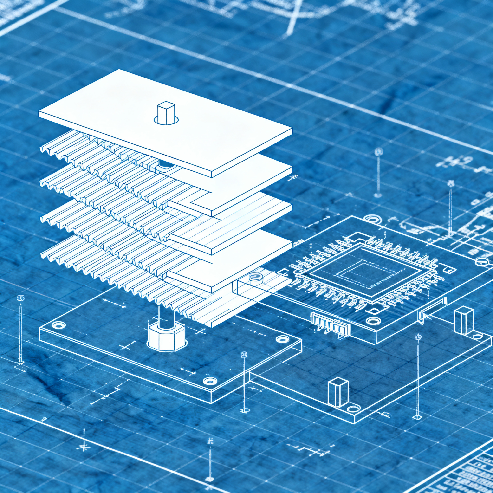
The first patent describes a patch antenna with a 3D-printed dielectric formed by overlapping inclined fins. Each fin has a thickness, an angle of inclination, and a precise distance from the adjacent fins. Controlled air spaces remain between one fin and the other.
This approach allows for lowering the effective permittivity of the material compared to the bulk. In practice: less transmission loss and greater control over signal propagation. The patent specifies that the angle, pitch, and thickness of the fins are chosen to ensure uniformity: along any vertical line through the structure, the amount of material and air remains constant.
- Weight reduction compared to traditional solid dielectrics
- Control of effective permittivity through print geometry
- Ability to customize the structure for specific frequencies and applications
The component is designed to be produced with standard additive manufacturing techniques. No special hardware is needed: just a professional 3D printer and composite materials already available on the market. The antenna can be used in wireless systems where reduced weight and high gain are priorities.
Horizon Microtechnologies has already worked on micro-printed RF components coated with silver or copper. The company indicates conductivity greater than 50% compared to solid copper, with coating thicknesses of 2-3 micrometers. This confirms that the technology is already applicable in real-world contexts.
Custom EMI shielding directly in the circuit
New metal deposition techniques allow for the integration of electromagnetic shields in semiconductor packages.
The second patent proposes a solution to protect integrated circuits from electromagnetic interference (EMI). The shielding structure is realized via 3D metal deposition directly between the package connectors, such as the balls of a ball grid array.
Instead of using standard shields, the method allows for the construction of custom metal walls around the critical points of the circuit. This reduces the occupied space and increases the functional density of the device. The shielding is integrated into the packaging process, without the need for additional external components.
| Appearance | Traditional screening | 3D screening |
|---|---|---|
| Customization | Limited to standard formats | Custom geometry |
| Integration | Separate component | Direct deposition in the package |
| Space occupied | Greater footprint | Reduced |
3D metal deposition techniques are already used in advanced electronics. The patent does not specify the materials, but copper and silver are common candidates for this type of application. The main challenge remains the conductivity and homogeneity of the deposited material.
A practical example: in an electronic packaging company, a production cell could 3D print shielding around ball grid arrays, improving the reliability of high-frequency devices. This type of solution is particularly useful for radar, satellite communications, and next-generation wireless infrastructures.
Trade-offs and limits
Despite tangible benefits, new solutions must overcome critical issues regarding materials, repeatability, and serial integration.
Both patents present interesting solutions, but not without uncertainties. For low-density antennas, the long-term stability of printed materials remains an open issue. Structures with controlled air gaps must maintain electrical properties even after thermal cycles, vibrations, and aging.
Repeatability is another challenge. Replicating the exact geometry in serial production requires tight control over printing parameters: temperature, speed, and layer orientation. Small variations can modify the effective permittivity and, consequently, the antenna's performance.
Low-density materials printed in 3D must demonstrate stability under real operating conditions: temperature, humidity, and mechanical stress. Not all geometries perform well in high-speed industrial environments.
For EMI shielding, the main problem is the conductivity of the deposited material. If the metal is not homogeneous or presents discontinuities, the shielding effectiveness decreases. Furthermore, integrating 3D deposition into high-speed production lines requires adaptations in existing processes.
Telemeter Electronic has proposed a printable filament for radar absorbers in the 76–81 GHz band. The company emphasizes that results must be experimentally validated on its own test bench, because anisotropy, roughness, and batch-to-batch repeatability can vary. This also applies to antennas and shielding: the difficult part is not printing the part, but ensuring it performs well under operating conditions.
Another aspect concerns costs. 3D printing is cost-effective for prototypes and small series, but for high volumes, traditional methods can still be more competitive. The challenge is finding the right balance: where customization and weight reduction justify the additional cost of the additive process.
Conclusion
3D printing opens concrete scenarios for more performant RF components and shielding. Antennas with low-density dielectrics and EMI shielding integrated into packages are solutions already achievable with existing technologies. The benefits in terms of weight, efficiency, and customization are tangible.
There is still room for development regarding materials, repeatability, and industrial scalability. But the direction is clear: additive manufacturing does not replace traditional methods; it accompanies them with more efficient hybrid solutions. For those working on radar, satellite communications, or high-frequency devices, it is time to evaluate the integration of these technologies into their projects.
article written with the help of artificial intelligence systems
Q&A
- What are the main advantages of RF antennas made with 3D technology?
- 3D antennas offer weight reduction compared to traditional solid dielectrics, better control of effective permittivity, and the ability to customize the structure for specific frequencies. Furthermore, they allow for greater efficiency thanks to reduced transmission losses.
- How does the low-density dielectric described in the first patent work?
- The dielectric is formed by overlapping inclined lamellae with controlled air gaps between them. This design allows for a reduction in effective permittivity compared to the bulk material, improving signal efficiency and maintaining uniformity in material distribution.
- What is the innovation introduced by the second patent on EMI shielding?
- The patent proposes 3D-printed EMI shields directly inside electronic packages, between the connectors of the ball grid array. This approach allows for the creation of custom shields, reducing occupied space and increasing the functional density of the device.
- What materials are used for the 3D printing of RF components according to the article?
- The article mentions the use of composite materials already available on the market, such as printable filaments and metals like copper and silver for metal deposition. Horizon Microtechnologies has achieved good results with copper or silver coatings on micro-printed components.
- What are the main challenges related to the mass production of these 3D components?
- The main challenges include the repeatability of geometry during production, the stability of materials over time, and the conductivity of deposited metals. It is necessary to maintain high precision in printing parameters to ensure constant performance.