Hybrid 3D Printing: How Does In Situ Electrodeposition Work?
Research from the Polytechnic University of Bari shows how electrodeposition can be integrated directly into 3D printing to create hybrid electronic components without resorting to separate or complex processes.
Real-time electrodeposition
The core of the process is the simultaneous deposition of copper during FDM printing, which enables integrated circuits in polymer substrates.
Researchers from the DMMM Department of the Polytechnic University of Bari have developed an electrodeposition head compatible with low-cost desktop printers. The system was tested on a Bambu Lab A1 using standard PLA filament and Protopasta CPLA.
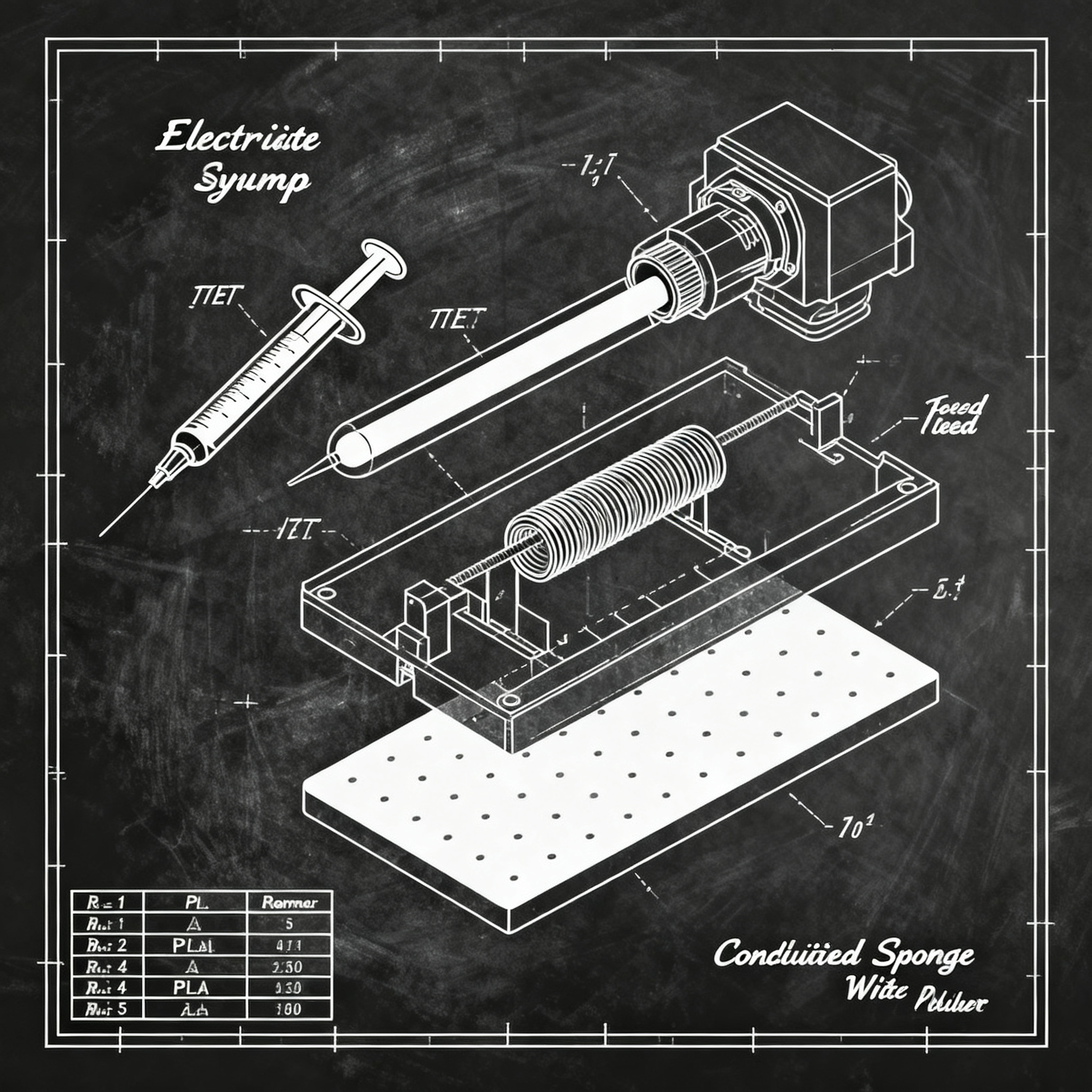
The head works through a simple but effective mechanism. A power supply controls a syringe piston that pumps the electrolytic solution through a PTFE tube. The liquid passes through a copper coil and reaches a sponge on the head, connected via a luer lock to a brush. While the normal head prints the polymer, the electrodeposition head deposits copper in the designated areas.
- Electrodeposition head compatible with low-cost desktop printers
- Simultaneous copper deposition during standard FDM printing
- Process controlled via custom G-code
- Creation of hybrid polymer-copper structures in a single session
The team developed a specific G-code to coordinate polymer printing with electroplating. This eliminates the need for separate processes that require manual handling and dedicated equipment. The electrolytic solution is activated only when necessary, reducing waste and complexity.
DIY hybrid electronic components
Sensors and conductive traces can be made directly on printed objects, opening new possibilities for proximity electronics.
The research group tested the system by creating strain sensors and working circuits. Conductive traces are deposited directly onto the polymer substrate during part construction, creating a true hybrid metal-polymer structure.
This capability represents a significant shift from traditional methods. Separate electroplating requires surface preparation, chemical baths, waiting times, and handling of potentially hazardous materials. The in-situ process reduces these steps to a simple printing operation.
Electroplating creates functional conductive traces for basic electronics, but does not replace the performance of high-precision industrial metallization. Electrical resistance is higher compared to traces made with professional methods.
Immediate applications include custom sensors, simple actuators, prototype circuits, and electronic components integrated into functional objects. For makers, this means being able to create complete electronic devices without having to resort to separate PCBs or complex assembly processes.
Limits and potential for makers
Although it does not replace industrial solutions, this technique offers direct access to electrical conduction in the hobbyist field.
Desktop electroplating has clear limits. The components are lighter than they appear because the metal is only a surface coating. Mechanical performance does not match that of solid metal parts. Environmental resistance is limited compared to industrial metallizations.
The process remains delicate and requires attention. The quality of the deposition depends on parameters such as electrolyte concentration, movement speed, applied current, and surface cleanliness. Small variations can compromise the adhesion or continuity of the traces.
However, for hobbyist applications and functional prototypes, the system offers concrete advantages. It eliminates the need for expensive specialized equipment, reduces exposure to hazardous chemicals, and simplifies the workflow by integrating metallization and printing into a single machine.
Other projects have attempted similar approaches. RobotFactory had developed desktop electrodeposition devices to be used with 3D printers, but they still required separate steps. The maker Dzingof has extensively experimented with the Metalizzr project. The novelty of the Italian research lies in the complete integration of the process.
Conclusion
In-situ electrodeposition represents an evolutionary step for accessible hybrid 3D printing, without requiring complex infrastructure. The system developed by the Polytechnic University of Bari demonstrates that it is possible to create functional electronic components on economical desktop printers.
The technology does not compete with industrial solutions for precision or performance, but for makers, educational labs, rapid prototyping, and small custom productions, it offers a direct path to integrated electronics.
Explore the first open-source projects that integrate this technique and experiment with creating circuits directly on your printer. The publication in Advanced Materials Technologies provides complete technical details for those who wish to replicate the system.
article written with the help of artificial intelligence systems
Q&A
How does the electrodeposition printhead developed by the Polytechnic University of Bari work?
The printhead uses a power supply that drives a syringe piston to pump the electrolytic solution through a PTFE tube. The liquid passes through a copper coil and reaches a sponge connected to a brush on the printhead. While the standard printhead deposits the polymer, the electrodeposition one deposits copper in the designated areas of the part.
What advantages does in-situ electrodeposition offer compared to traditional methods?
The process eliminates the need for separate steps, surface preparation, chemical baths, and dedicated equipment. The entire procedure takes place in a single printing session controlled via custom G-code, reducing waste, complexity, and exposure to hazardous chemicals.
On which printers and materials has the system been tested?
The system was tested on an affordable desktop Bambu Lab A1 printer. Standard PLA and Protopasta CPLA filaments were used as polymeric substrates for the deposition of conductive traces.
What electronic applications can be realized with this technique?
It is possible to create custom sensors, simple actuators, conductive traces, and prototype circuits directly on printed objects. This allows integrated electronic components to be produced without resorting to separate PCBs or complex assembly processes.
What are the main limitations of desktop electrodeposition for makers?
The metal constitutes only a surface coating, so mechanical performance and environmental resistance do not match those of solid metal parts or industrial metallizations. Furthermore, deposition quality depends on delicate parameters such as electrolyte concentration and applied current.
What is the novelty of this research compared to other similar projects?
Unlike previous approaches such as those by RobotFactory or Dzingof's Metalizzr project, which required separate steps, the novelty of the Italian research lies in the complete integration of the process. Electrodeposition occurs simultaneously with FDM printing in a single affordable desktop machine.