Aerosol Jet Printing: Really Revolutionary?
Transistors produced with Aerosol Jet Printing are overcoming old limits of printed electronics, opening new paths for flexible and low-cost devices.
German researchers have demonstrated transistors printed with aerosol jet technology capable of withstanding thousands of switching cycles without functional degradation. This result marks the transition from simple demonstrative prototypes to devices ready for concrete industrial applications such as sensors, large-area logic circuits, and flexible electronics.
AJP technology allows for the deposition of conductive and semiconductive materials on plastic substrates, glass, and non-planar surfaces. It reduces costs and complexity compared to traditional silicon-based microelectronics.
Precision and resolution: where does AJP fit?
Aerosol jet printing achieves resolutions between 10 and 50 micrometers, positioning itself as an interesting compromise between geometric flexibility and productivity.
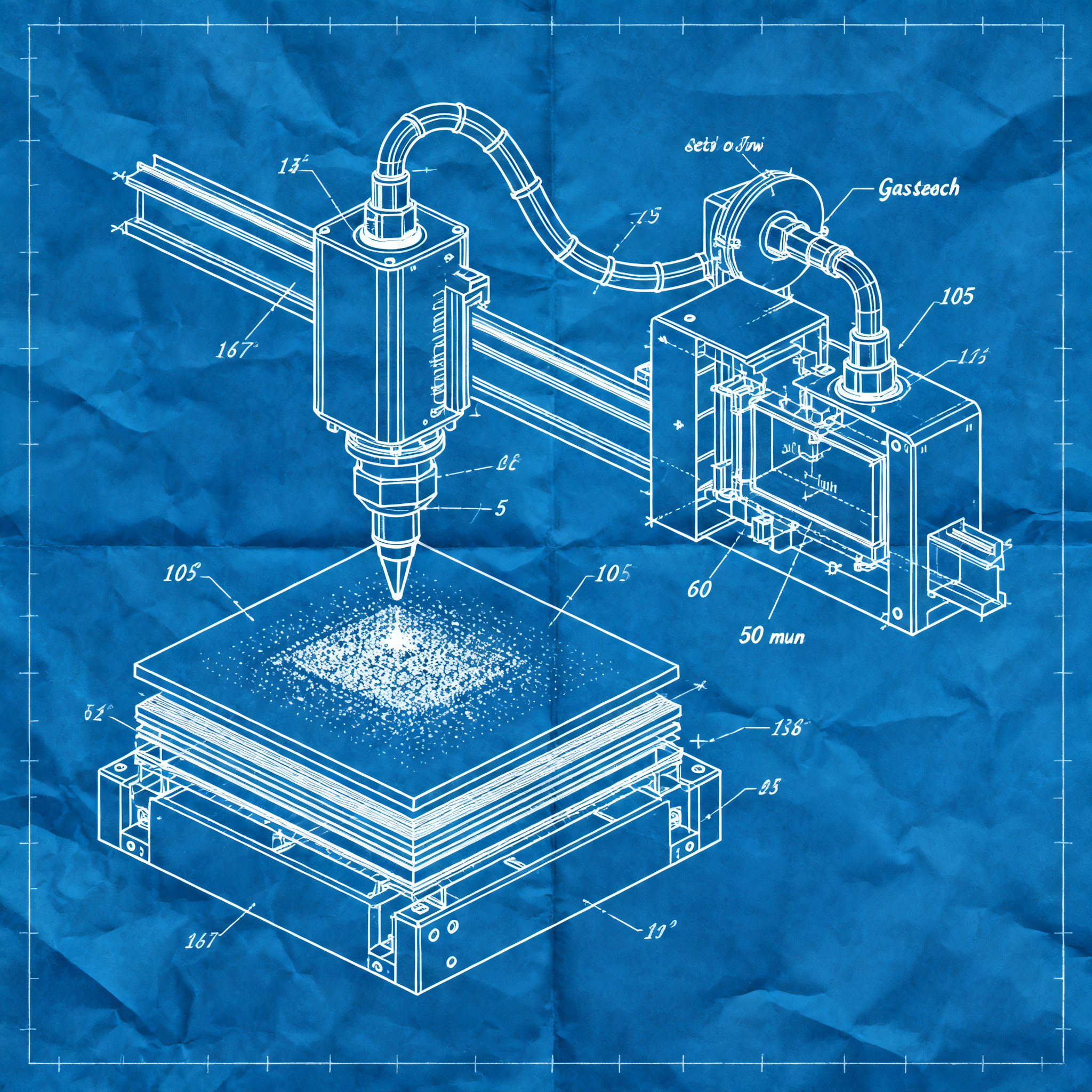
Aerosol Jet Printing nebulizes a functional ink into an aerosol, conveying it towards a nozzle where a sheath gas flow focuses the jet. Unlike classic inkjet, the material can also be deposited on three-dimensional surfaces with controlled thicknesses.
The typical width of printed lines varies between 10 and 50 micrometers. Multiple thicknesses are obtained by overlapping successive passes. This resolution does not reach the nanometric levels of silicon microelectronics, but proves adequate for devices that require fine geometries without extreme miniaturization.
| Technology | Typical resolution | Compatible surfaces | Process temperature |
|---|---|---|---|
| Aerosol Jet Printing | 10–50 µm | Planar and 3D | Moderate (compatible polymers) |
| Traditional Inkjet | 20–100 µm | Mainly planar | Low-moderate |
| Silicon lithography | <10 nm | Planar only | High |
The process operates at moderate temperatures, compatible with flexible polymer substrates. This opens possibilities for wearable electronics, conformable sensors, and integrated circuits directly on mechanical components.
Materials comparison: who can ‘fly’ in the Aerosol Jet?
AJP transistors use combinations of conductive, dielectric, and semiconductor materials deposited in sequence, with post-treatments by heat or plasma to optimize performance and adhesion.
Printed thin-film transistors (TFTs) require multiple functional layers: source, drain, and gate electrodes, gate dielectric, and semiconductor. Each layer is deposited on an insulating substrate using digital printing techniques.
The combination of controlled deposition and post-treatments optimizes the microstructure of the channel and the adhesion between layers. This reduces defects and traps that would compromise reliability under repeated cycling.
- Nanoparticle-based conductive inks (typically silver)
- Organic and inorganic colloidal semiconducting materials
- Printable dielectrics for gate isolation
- Conductive pastes for electrodes and interconnections
Other research groups work on transistors printed with nanocrystal-based inks, deposited via spin-coating or inkjet. The common goal is to realize the entire device with printable colloidal materials, paving the way for logic circuits, flexible displays and integrated sensors on large areas.
Reliability over time: real resistance of printed transistors
Reliability tests show that AJP transistors maintain stable electrical characteristics for thousands of switching cycles, overcoming the typical limits of printed organic devices.
Reliability tests involve the repeated application of voltage pulses to the gate. The variation of drain current, threshold voltage and on/off ratio over time is measured.
In many printed organic devices these quantities tend to degrade rapidly. Causes include charge traps, interfacial instability and ion migration. The German transistors limit these phenomena through careful choice of materials and optimized deposition sequence.
This level of performance brings printed transistors beyond the proof of concept, bringing them closer to real-use conditions in sensors that must function for long periods or in large-area printed logic circuits that require reliable operability.
Repeatable behavior over numerous switching cycles represents a fundamental requirement for industrial applications. Without this stability, devices remain confined to laboratory demonstrations without concrete commercial outlets.
Scalability vs. traditional: when is it really convenient?
Aerosol jet printing offers economic and production flexibility advantages when the integration density of silicon microelectronics is not required, but scalable processes on low-cost substrates are needed.
In many application scenarios, it is not necessary to reach silicon integration density. Instead, it becomes essential to combine good electrical reliability with scalable fabrication processes, on low-cost and low-temperature substrates.
AJP represents an interesting compromise between resolution, geometric flexibility, and productivity. This is especially true when the technology is integrated into automated lines for large-area production.
The main challenge remains standardization. Shared guidelines are needed for materials, process parameters, and reliability tests. Only in this way can printed transistors be qualified with uniform criteria and accepted by the industry.
When to choose AJP over silicon
- Evaluate the required density: If geometries under 10 µm are needed, silicon remains necessary.
- Consider the substrate: Flexible, curved, or non-planar surfaces favor AJP.
- Analyze volumes: Distributed production and customization push towards digital printing.
- Check costs: For large areas and medium-low volumes, AJP may be more economical.
The integration between AJP, other 3D printing techniques, and material recycling processes could lead to a new generation of additive electronic devices. These would be designed from the outset for distributed production and end-of-life recovery.
Conclusion
Aerosol Jet Printing is demonstrating concrete potential in the field of printed electronics. Transistors that withstand thousands of cycles without degradation mark an important step towards real industrial applications.
The true limits of the technology emerge when putting materials, precision, and scalability to the test. The resolution of 10–50 micrometers is sufficient for many applications, but not for all. Compatibility with flexible substrates opens new markets, but requires process standardization.
Do you want to understand if AJP can work for your project? Deepen the technological data and compare them with your specific needs for resolution, reliability, and production costs.
article written with the help of artificial intelligence systems
Q&A
What are the main advantages of Aerosol Jet Printing compared to traditional microelectronics?
Aerosol Jet Printing allows printing on flexible and non-planar substrates, operating at moderate temperatures. This reduces costs and complexity compared to traditional silicon-based processes.
What is the typical resolution of Aerosol Jet Printing and how does it compare to other technologies?
The resolution of AJP ranges between 10 and 50 micrometers, positioning it between traditional inkjet and silicon lithography. It does not achieve nanometric miniaturization but is sufficient for many applications.
What materials can be used in aerosol jet printing?
Conductive inks based on nanoparticles, organic and inorganic semiconductor materials, printable dielectrics, and conductive pastes for electrodes and interconnections can be used.
Why does the reliability of printed transistors represent a breakthrough for industrial applications?
AJP transistors show electrical stability for thousands of switching cycles, overcoming the limitations of printed organic devices. This makes them suitable for sensors and large-scale logic circuits.
In which cases is it convenient to choose Aerosol Jet Printing over silicon?
AJP is convenient when extreme miniaturization is not required, but flexible substrates, low-cost scalable production, and distributed customization are needed.