Additive Manufacturing in Semiconductor Packaging: The Operational Plan of XTPL and Manz Asia
The integration of additive manufacturing into advanced packaging processes is no longer a future bet, but an industrial reality driven by targeted partnerships such as the one between XTPL and Manz Asia. XTPL’s Ultra-Precise Dispensing (UPD) technology is entering the production flows of semiconductor industry leaders, marking a paradigm shift toward more flexible and higher-performing processes. The strategic collaboration with Manz Asia allows the Polish company to scale adoption of its technology without direct infrastructure investments, transforming a machinery sale into a technology demonstrator in the world’s most important market for semiconductors.
Definition and Functionality of Advanced Packaging
Advanced packaging evolves from a simple protective enclosure to an active component in integrated circuits, enabling 3D configurations and superior performance through functional integration.
Chip packaging includes all components of a semiconductor device except the die (the “chip” itself). As IBM explains, “packaging provides the mechanical environment in which a chip operates.” Advanced packaging stands out because the components that house the chip not only provide protection, but become an integral part of the device’s functionality itself.
Progress in this field stems from the 3D design revolution in semiconductors over the past twenty years. Manufacturers began exploring the advantages of vertically stacking chips instead of traditional side-by-side placement. This evolution has made the integration of additive manufacturing increasingly common in advanced packaging conversations, supporting the business models of companies such as Poland’s XTPL.
The shift from 2D to 3D has completely transformed the way semiconductor devices are designed. System in a Package (SiP) architectures, which combine several smaller dies in the same device with advanced packaging, are becoming strategic in global semiconductor competition, so much so that China has developed significant capabilities in this area to offset restrictions on equipment imports.
The Role of Additive Manufacturing in Electronics
Additive techniques enable micrometric precision and rapid customization, ideal for complex substrates and advanced interconnections that traditional packaging struggles to achieve.
Additive manufacturing for electronics (AME) covers a wide range of applications, from RF antennas to rapidly iterated PCB prototypes. Among these, advanced chip packaging probably represents the most significant growth opportunity for the AME segment. The ability to move from 2D to 2.5D and 3D design has revolutionized chiplets, semiconductor devices composed of small chip systems instead of integrating all functions into a single die.
The additive approach makes it possible to create conductive structures, three-dimensional interconnects, and sensor integrations directly on the package, reducing dependence on conventional substrates and on traditional high-complexity packaging lines. This translates into greater geometric flexibility and the possibility of reducing the number of dedicated masks and photolithographies.
AME platforms allow working on rigid and flexible substrates, with geometries not constrained to standard packages. This approach makes it possible to integrate signal lines, power planes, and three-dimensional interconnects directly into the body of the package or module, reducing the number of steps compared with solutions based on multilayer PCBs and conventional organic substrates.
XTPL and Ultra-Precise Dispensing Technology
XTPL's UPD solution enables sub-micron controlled depositions, essential for high-density applications in advanced electronics and complex packages.
XTPL has developed a microscopic 3D printing technology that makes it possible to deposit conductive materials in the form of lines and structures with widths on the order of a few micrometers. Unlike conventional inkjet or screen printing, the solution combines accurate control of ink flow with extremely precise positioning, achieving narrow, uniform, high-aspect-ratio traces.
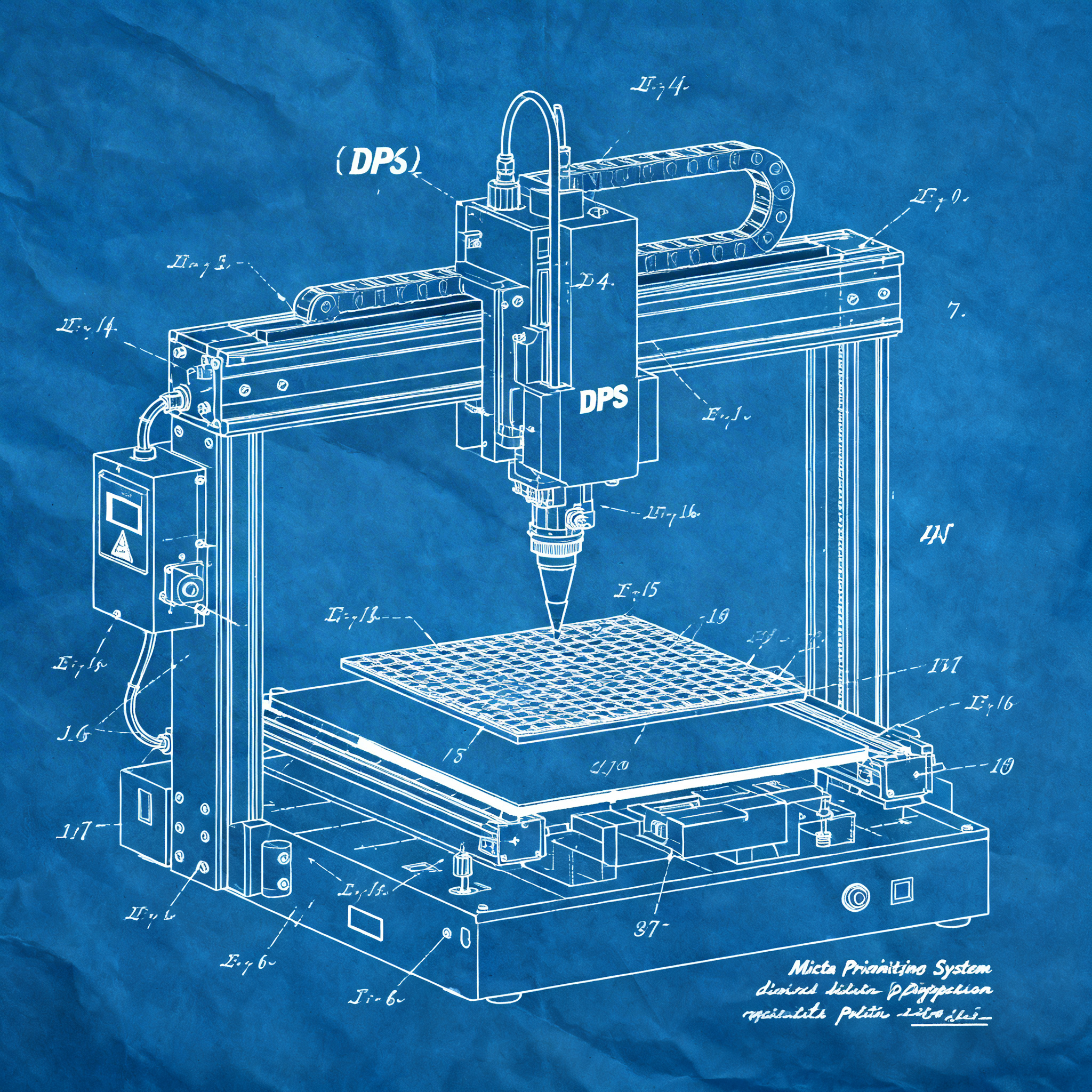
This type of deposition is particularly relevant for advanced electronics, where miniaturization requires very dense interconnects with stringent requirements on electrical resistance, adhesion to substrates, and compatibility with subsequent packaging stages. XTPL's Delta Printing System (DPS) leverages UPD technology for applications ranging from advanced packaging to high-density interconnects.
As the number of I/Os and bandwidth increase in modern devices, thermal management and signal routing over very short distances become critical. Traditional techniques based on bumps, wire bonding, or micro-vias encounter density and cost limits in some configurations, opening up space for additive deposition processes that make it possible to create custom bridges, lines, and vertical connections directly on the package.
Partnership Strategy with Manz Asia
Collaborating with Manz Asia allows XTPL to integrate its technology into existing production flows without having to build dedicated facilities, accelerating access to the Taiwanese market.
XTPL has announced a strategic partnership with Manz Asia, a semiconductor equipment manufacturer specializing in advanced packaging technologies that maximize chip performance. The starting point of the collaboration is Manz Asia's acquisition of an XTPL Delta Printing System (DPS) unit, which leverages Ultra-Precise Dispensing technology.
The acquisition will be installed in the first half of the year at the Manz Semiconductor Innovation R&D Center in Taiwan, enabling XTPL to reach a completely new audience while Manz Asia gains a new process capability. Since the printhead is the key to the UPD technique, XTPL emphasizes that the strategic partnership provides a potential path to ultimately integrate XTPL's printhead into Manz Asia's machines.
By collaborating with Manz Asia, XTPL has achieved the goal of expanding its physical sales positions in key markets without having to commit the capital needed to expand that presence independently, turning a machine sale into a technology demonstrator in the world's most important semiconductor market.
Robert Lin, CEO of Manz Asia, said: “This strategic partnership with XTPL expands our printing capabilities in ultra-precise material deposition, enabling a wide range of advanced semiconductor applications. The technology supports conductive and non-conductive materials on 2D, 2.5D, and 3D substrates in various production scenarios.”
Operational Cases and Industrial Scalability
Pilot projects demonstrate the large-scale applicability of UPD technology in complex, certified production environments, with a roadmap toward volume production.
XTPL has also announced a strategic partnership with a major semiconductor industry OEM for an advanced packaging solution based on its 3D printing technology. The agreement includes joint validation phases, integration of the XTPL module into the manufacturer's lines, and a roadmap toward large-scale production once performance and reliability targets are met.
In the initial phase, the teams define use cases with pitch, thickness, and electrical resistance requirements compatible with the OEM's product roadmaps, including reliability tests such as thermal cycling, humidity, and accelerated aging. Once the solution is validated, the goal is to achieve in-line integration, in which XTPL modules interface with existing equipment while coordinating with other process steps.
For XTPL, this means entering the supply chain of a major player on a stable basis, with the prospect of recurring revenue tied to systems, maintenance, and consumables. Filip Granek, CEO of XTPL, commented: “I am excited to launch the partnership with Manz Asia, a company with a strong position and deep experience in the semiconductor industry in Taiwan and Asia. The synergy between XTPL's ultra-precise dispensing technology and Manz Asia's expertise in advanced semiconductor packaging is a natural combination.”
The expansion into Taiwan could be precisely what gives the company a long-term advantage in the United States and Europe. If the company can demonstrate its technology in the global semiconductor sector, there is a good chance that Taiwanese semiconductor manufacturers will turn to UPD technology as they consolidate their generational investments in production capacity on the North American and European continents.
Conclusion
The implementation of additive manufacturing in the semiconductor sector marks an epochal shift toward more flexible and higher-performing processes, with impacts on supply chain resilience.
Advanced packaging is today one of the most dynamic sectors in the semiconductor industry, and the integration of additive technologies such as XTPL's Ultra-Precise Dispensing is demonstrating that additive manufacturing can move from prototyping to industrial production even in the most demanding contexts. The partnership with Manz Asia illustrates an effective operating model: instead of building its own infrastructure, XTPL integrates its technology into the production flows of established partners, accelerating adoption and reducing risks.
This collaborative approach could become a model for other companies in the AME sector that are seeking to scale their technologies without the enormous capital investments typically required by the semiconductor industry. With the growing importance of chiplets and 3D architectures, demand for flexible and high-precision packaging solutions is set to increase.
Find out more about how companies are already transforming their production lines with precision additive technologies and discover which other players are emerging in this rapidly evolving space, where the convergence of additive manufacturing and advanced electronics is redefining the boundaries of what is possible in device miniaturization and performance.
article written with the help of artificial intelligence systems
Q&A
What is the main objective of the partnership between XTPL and Manz Asia in the semiconductor sector?
The main objective is to integrate XTPL's Ultra-Precise Dispensing (UPD) technology into Manz Asia's advanced packaging processes, scaling the adoption of the technology without direct infrastructure investments. This allows XTPL to enter the Taiwanese semiconductor market through a technological demonstrator.
What does XTPL's Ultra-Precise Dispensing (UPD) technology consist of?
The UPD technology enables controlled depositions at the sub-micron level, essential for high-density applications in advanced electronics. Unlike traditional techniques, it allows the creation of conductive lines and structures with micrometric precision, improving interconnections and direct integration in packages.
How is the concept of packaging changing in the semiconductor industry?
Advanced packaging is no longer just a protective casing but an active component contributing to the integrated circuit's functionality. Thanks to 3D design and functional integration, superior performance and more compact configurations can be achieved, such as in System in a Package (SiP) systems.
What advantages does additive manufacturing offer compared to traditional methods in electronic packaging?
Additive manufacturing provides greater precision, geometric flexibility, and a reduction in the number of masks and photolithography steps. It enables the realization of three-dimensional interconnections and integrated structures directly on the package, overcoming the limitations of traditional techniques like bump or wire bonding.
What is the role of the Delta Printing System (DPS) in XTPL's strategy?
The DPS is the system that implements XTPL's UPD technology and represents the core of the collaboration with Manz Asia. It is installed in the R&D centers of partners to demonstrate its effectiveness and prepare for large-scale integration into existing industrial processes.