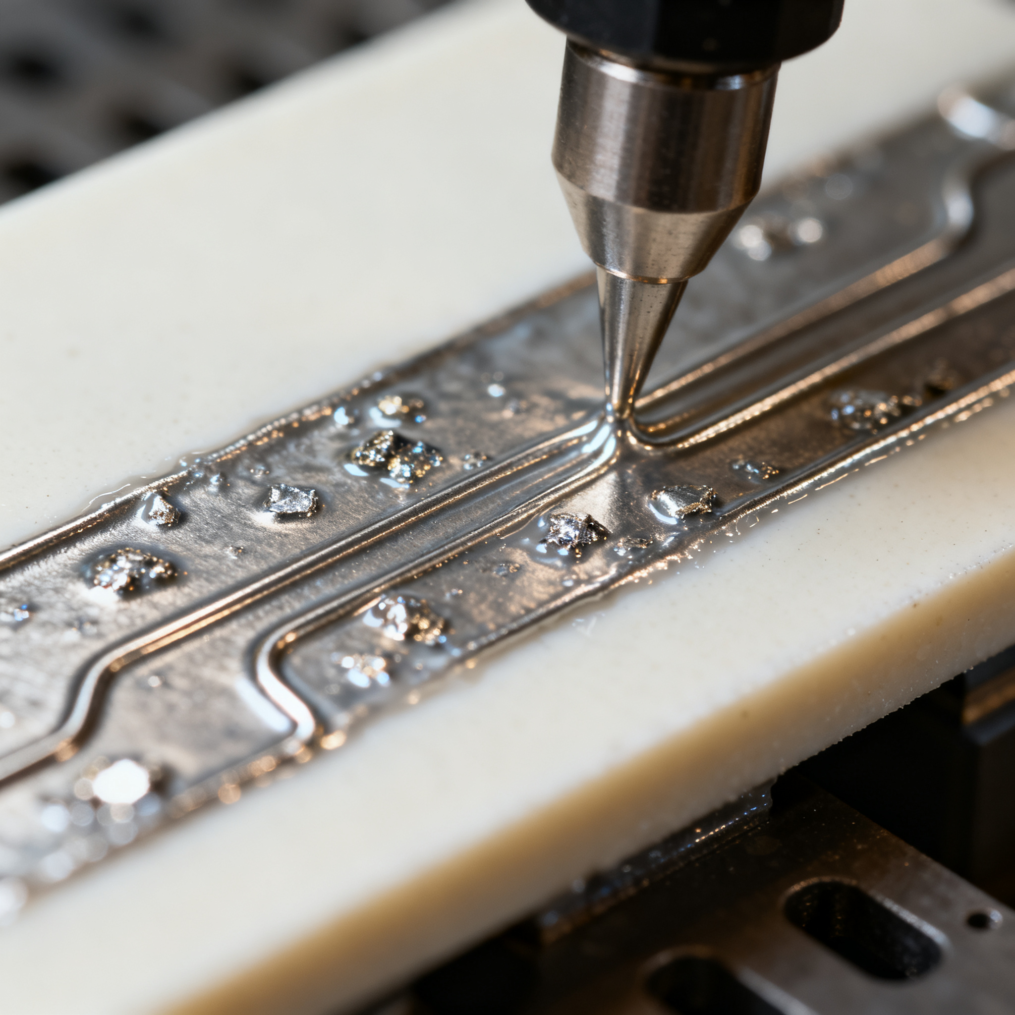
3D printing that conducts electricity?
Additive manufacturing is no longer limited to shape: two emerging patents show how it is possible to directly build circuits and shielding inside devices, reducing steps and costs.
- SYSTEM AND METHOD FOR ELECTROCHEMICAL ADDITIVE MANUFACTURING — September 4, 2025
- 3D ELECTROMAGNETIC INTERFERENCE SHIELDING STRUCTURE FOR SEMICONDUCTOR DEVICE — March 4, 2026
Integrating electrical functions into a printed component is no longer a laboratory experiment. Two recent patents describe concrete methods for building conductive traces and shielding directly during additive manufacturing. No subsequent assemblies, no manual gluing.
The first patent uses an electrochemical process to deposit conductive materials on thermally active substrates. The second prints three-dimensional metal structures in electronic packages to block electromagnetic interference. Both aim to simplify the supply chain and improve performance.
Circuiti dentro l’oggetto: come funziona
Un approccio elettrochimico permette di costruire componenti conduttivi direttamente su substrati attivi, migliorando l’integrazione termica ed elettrica.
The patent “SYSTEM AND METHOD FOR ELECTROCHEMICAL ADDITIVE MANUFACTURING” describes a composite structure that forms on a thermally dissipative substrate. The process deposits a conductive attack layer, then builds on top an electrochemical matrix containing solid inclusions.
The inclusions can be metallic or non-metallic particles with high thermal conductivity. The matrix that binds them is also metallic. The result is a component that conducts heat and electricity more efficiently than traditional structures.
- Improvement of thermal conduction thanks to high conductivity inclusions
- Reduction of assembly steps
- Greater repeatability of the production process
The patent does not specify exact values of conductivity or operating temperatures, but clearly indicates the application: components that must dissipate heat while carrying current. Integrated heat sinks with electrical traces, for example.
An electric vehicle inverter manufacturer could directly print heat sinks with embedded conductive traces. Fewer solder joints means fewer thermal failure points. Fewer assemblies means less batch-to-batch variability.
EMI shielding without glue or solder
3D printing of integrated metal structures in packages simplifies assembly and improves electromagnetic performance.
The patent “3D ELECTROMAGNETIC INTERFERENCE SHIELDING STRUCTURE FOR SEMICONDUCTOR DEVICE” proposes printing metal walls directly between the connectors of an electronic package. The structure is formed by 3D deposition during device manufacturing.
Today, EMI shields are often metal sheets or covers assembled by hand or with pick-and-place. This patent eliminates that step. The shielding wall grows together with the package, following the geometry of the connectors.
The main advantage is conformability: the shielding can follow complex profiles without the need for dedicated tools. This opens up more compact geometries and better coverage of critical areas.
Integration process
- Package deposition: the substrate and connectors are formed using standard techniques.
- 3D printing of the metal wall: a deposition head deposits conductive material between the elementary connectors.
- Finishing: the complete device is sealed without additional assembly steps.
An automotive sensor manufacturer could print EMI shields directly into chip packages. Fewer components to manage, less scrap from testing, less machine time. The patent does not provide data on conductivity or minimum thicknesses, but the logic is clear: fewer steps, fewer errors.
Real advantages, adoption near
Both technologies offer tangible benefits and are compatible with existing production processes.
The electrochemical patent fits into production lines that already use additive deposition on metal or ceramic substrates. It does not require exotic materials: the inclusions can be standard high-conductivity particles. Repeatability depends on control of the electrochemical process, but the principle is well-established.
The EMI shielding patent relies on already mature 3D metal printing techniques. The novelty is the application: integrating the shield into the package instead of assembling it later. This reduces component costs and simplifies logistics.
| Appearance | Traditional method | Additive method |
|---|---|---|
| Assembly steps | Multiple (deposition + assembly + fixing) | Single (integrated deposition) |
| Geometric conformity | Limited to standard shapes | High, follows the package profile |
| Thermal management | Separate joints, higher thermal resistance | Direct integration, fewer interfaces |
Both patents indicate applications in power electronics and automotive, sectors where thermal reliability and cost reduction are concrete priorities. These are not distant promises: the described processes are compatible with already available AM technologies.
Trade-offs and limitations
Despite the advantages, there remain critical issues related to material durability and initial equipment costs.
The electrochemical patent does not provide data on the durability of bonds between matrix and inclusions. In automotive or industrial applications, thermal cycles and vibrations can stress the interfaces. Field validation is necessary before large-scale adoption.
The durability of electrochemical bonds under real operating conditions is not yet documented. Initial costs for specialized equipment can be a barrier for small-scale manufacturers.
The EMI shielding patent does not specify how to ensure uniformity of conductivity in printed structures. Local variations could compromise shielding effectiveness. Compatibility with packaging thermal cycles also remains to be verified: some sealing processes reach high temperatures.
Both patents require investments in dedicated equipment. For the electrochemical process, a deposition control system is needed. For metal 3D printing, a print head compatible with conductive materials is needed. These are not prohibitive costs, but neither are they negligible for existing lines.
Direct integration of electronic functionalities into 3D printing is no longer science fiction: it is a reality within reach of the production line. The two patents show concrete paths to reduce assemblies, improve thermal performance, and simplify the management of electromagnetic interference.
The most immediate applications are in power electronics and automotive, where the reduction of assembly steps directly translates into reliability and costs. Durability and uniformity under real operating conditions remain to be validated, but the direction is set.
Segui i prossimi sviluppi di queste tecnologie: potrebbero ridefinire l’elettronica embedded nei prossimi anni.
article written with the help of artificial intelligence systems
Q&A
What does the patent "SYSTEM AND METHOD FOR ELECTROCHEMICAL ADDITIVE MANUFACTURING" enable?
It enables building conductive components directly onto thermally dissipative substrates by means of an electrochemical process. The method deposits a conductive layer and an electrochemical matrix containing solid inclusions with high thermal conductivity. The result is a component that conducts heat and electricity more efficiently than traditional structures.
What is the main advantage of the patent "3D ELECTROMAGNETIC INTERFERENCE SHIELDING STRUCTURE FOR SEMICONDUCTOR DEVICE"?
It enables printing metal walls directly between the connectors of an electronic package during production, eliminating the manual assembly of metal sheets or lids. The shielding can follow complex geometric profiles without dedicated tools, improving coverage of critical areas. This reduces component costs and simplifies production logistics.
In which sectors do these additive manufacturing technologies find their most immediate application?
The most immediate applications are in power electronics and the automotive sector. In these areas, the reduction of assembly steps translates directly into greater thermal reliability and lower production costs.
What are the main issues that still hinder the large-scale adoption of these patents?
The durability of electrochemical bonds under real operating conditions with thermal cycles and vibrations is not yet documented. In addition, the initial costs for specialized equipment represent a barrier for small manufacturers, and the uniformity of conductivity in printed structures remains to be verified.
How does the additive method differ from the traditional method in terms of thermal management and assembly?
The traditional method involves multiple soldered joints with higher thermal resistance and several assembly steps. The additive method directly integrates conductive and dissipative functions into the component, reducing interfaces and thermal failure points.