How the Plug-and-Play Optical Interface Made with 3D Printing Works
A new plug-and-play optical interface developed by German researchers enables high-efficiency connections between optical fibers and integrated photonic circuits thanks to the 3D printing of polymeric structures directly on the chip. The system, which reaches losses of only 0.78 dB, represents a significant advancement towards the modularization of photonic systems, comparable to the introduction of USB connection in electronics.
Integrated photonic circuits (PICs) use light to process information through nanometric waveguides, offering high data transmission capacity and low latency in applications ranging from sensing to optical communications, from quantum technologies to neuromorphic computing. However, the efficient connection between optical fibers and chips represents a crucial engineering challenge: fibers and on-chip waveguides present different modal field diameters, requiring interfaces that minimize optical losses while maintaining broadband transmission.
Principle of Vertical Coupling Operation
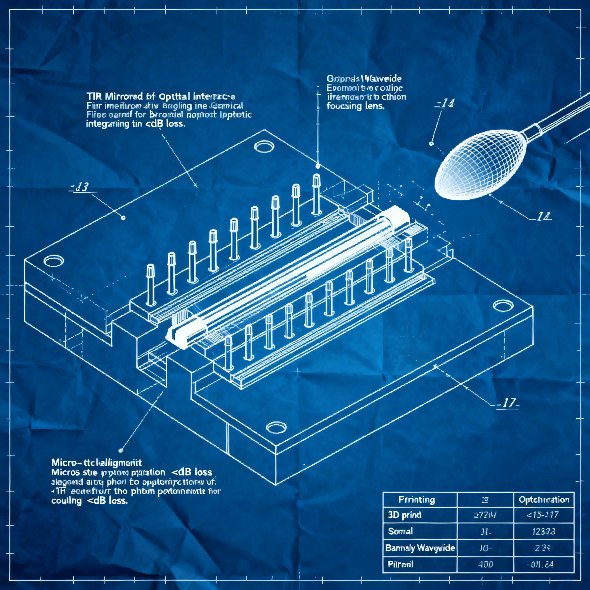
Optical coupling is based on polymeric structures that exploit total internal reflection to redirect light vertically from the fiber to the waveguides on the chip, through a geometry optimized by simulations.
The team led by Erik Jung of the University of Heidelberg, in collaboration with Wolfram Pernice of the University of Münster, developed out-of-plane couplers based on total internal reflection (TIR). These polymeric structures redirect light from the fiber vertically into the integrated waveguides on the chip.
The couplers incorporate several functional sections: a tapered modal transfer section that transfers optical power from silicon nitride (Si₃N₄) waveguides to polymeric waveguides, followed by a modal field expansion region, a TIR reflection surface and an ellipsoidal focusing lens that adapts the optical beam to the fiber mode. The geometry of the couplers was optimized using finite element simulations in the frequency domain.
Measurements demonstrate a peak transmission of -0.41 dB per coupler, corresponding to an optical transmission efficiency of about 91%. The broadband coupling performances remain stable on wavelengths from 1500 to 1600 nanometers, covering the S, C and L bands used in optical communication systems.
Two-Photon 3D Printing Technology
The fabrication process uses two-photon polymerization, a high-resolution 3D printing technique that employs femtosecond lasers to create polymeric microstructures directly on the chip surface.
The realization of optical microstructures occurs via two-photon polymerization, a nanometric 3D printing process that allows the construction of complex geometries with sub-micrometric precision. This technology uses ultrashort pulse lasers (femtoseconds) to induce the selective polymerization of photosensitive resins exclusively at the focal point of the laser beam.
The structures are printed directly onto the silicon nitride photonic platform, above the terminal regions of the waveguides. This process allows for the integration of complex optical elements – prisms, total internal reflection mirrors, and printed waveguides – into a single microstructure that acts as a coupling interface. This capability for direct additive fabrication eliminates the need for traditional active alignment processes, which require precise fiber positioning using actuators while monitoring the transmitted optical power in real time.
Mechanical Design and Physical Connectivity
The interface integrates 3D-printed alignment pins and uses standard MTP cables, ensuring compatibility with existing infrastructure and repeatable passive alignment without active positioning procedures.
The removable architecture is based on 3D-printed alignment pins and polymer couplers fabricated directly on the chip. A multifiber female cable with a push-on termination (MTP) connects to these printed structures, enabling passive alignment between the fiber array and the photonic chip. The authors describe this architecture as comparable to a USB connection for integrated photonic circuits, enabling repeatable connections without active alignment.
The alignment structures printed directly on the chip surface also eliminate the need to precisely position photonic chips relative to printed circuit boards during assembly. The system is designed to integrate with standard fiber arrays mounted in holders with alignment pins, a geometry already widespread in the telecommunications and optical interconnection industries.
The coupling method can be adapted to additional photonic platforms, including silicon-on-insulator, lithium niobate, and tantalum pentoxide, where only the waveguide transition region requires modifications.
Optical Loss and Performance Evaluation
The system achieves total coupling losses of 0.78 dB with stable performance across a wide spectral band, demonstrating repeatability and wider mechanical tolerances compared to traditional methods.
Total coupling losses of 0.78 dB represent a significant result for a removable, plug-and-play interface. This value includes losses through the entire coupling chain, from the optical fiber through the printed polymer structure to the waveguide on the chip.
Performance stability across the S, C, and L bands (1500–1600 nm) is particularly relevant for optical communication applications, where spectral bandwidth determines data transmission capacity. The interface partially compensates for mechanical misalignments and relaxes positioning tolerances, factors that in conventional production flows require slow, costly, and difficult-to-scale active alignment procedures for many channels.
Researchers have demonstrated the scalability of the concept by applying the interface to a neuromorphic photonic processor with 17 optical gates, where multiple light channels are processed in parallel to implement operations similar to those of neural networks. The interface allows for connecting multi-channel fiber arrays to the gate matrix on the chip in a repeatable manner, without having to manually align each individual fiber.
Conclusion
The 3D-printed plug-and-play optical interface represents a concrete progress towards modular and scalable photonic systems, maintaining high optical performance. The combination of low losses, broadband coupling, and reproducible passive alignment supports the development of larger photonic systems for computing and communication. Compatibility with different photonic platforms and integration with standard MTP cables make this solution particularly promising for the industrialization of integrated photonic circuits.
Explore the technical details of two-photon 3D printing in photonic devices and evaluate the industrial applicability of this solution for your applications in optical communication, sensing, or neuromorphic computing.
article written with the help of artificial intelligence systems
Q&A
- What is the main advantage of the plug-and-play optical interface made with 3D printing?
- The main advantage is enabling high-efficiency connections between optical fibers and integrated photonic circuits with very low losses (0.78 dB). This system eliminates the need for active fiber alignment, simplifying the connection process and improving repeatability.
- How does vertical coupling work in the new interface?
- Vertical coupling exploits polymeric structures that use total internal reflection (TIR) to redirect light from the optical fiber to the waveguides on the chip. It includes components such as ellipsoidal lenses and modal transfer sections to optimize light coupling.
- What characterizes the 3D printing technology used to create the interface?
- The technology employed is two-photon polymerization, which uses femtosecond lasers to create polymeric microstructures with sub-micrometric precision directly on the chip. This process allows for building complex geometries necessary for optical coupling without manual alignments.
- What are the practical implications of using MTP cables and 3D-printed alignment pins?
- Standard MTP cables and 3D-printed alignment pins ensure compatibility with existing infrastructure and allow for repeatable passive alignment. This simplifies integration into industrial systems and reduces costs associated with active fiber alignment.
- In which spectral bands does the interface maintain stable performance?
- Performance remains stable in the S, C, and L bands, ranging from 1500 to 1600 nanometers. This spectral width is crucial for high-capacity optical communication applications, where broad bandwidth is essential to maximize data transmission.